Tuesday, October 18, 2022

Direct Conversion Radio Receiver Using the MC1496 Double Balanced Modulator Demodulator IC

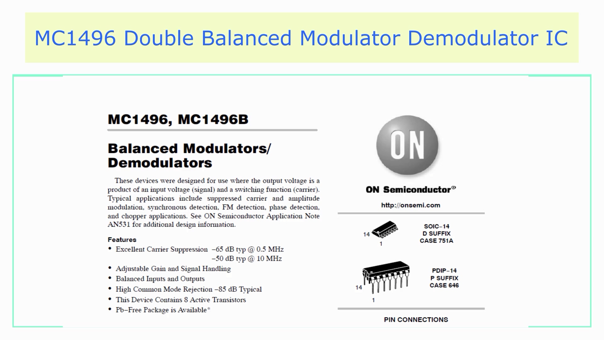
The MC1496 IC is a balanced modulator/demodulator IC used in various circuits for modulation or demodulation applications. It provides an output voltage, which is a product of an RF input from the antenna and a switching function through a carrier signal. This is a 14 pin IC, which is available as a dual inline or SOIC package.


The Important Features of MC1496 IC are
  1. It has excellent carrier suppression of typically -50dB at 10 MHz.
  2. Adjustable gain and signal handling characteristics.
  3. Balanced input and output circuits.
  4. High common mode rejection typically at -85 dB.
  5. This IC contains 8 active transistors.
 
Circuit Schematic of MC1496 IC
The inner circuit of the MC1496 IC consists of an upper quad differential amplifier driven by a standard differential amplifier with dual current sources. The output collectors are cross-coupled and therefore full-wave balanced multiplication of the two input voltages occurs. At the output, the collectors are terminated by two external load resistors or broadband transformers to the VCC.


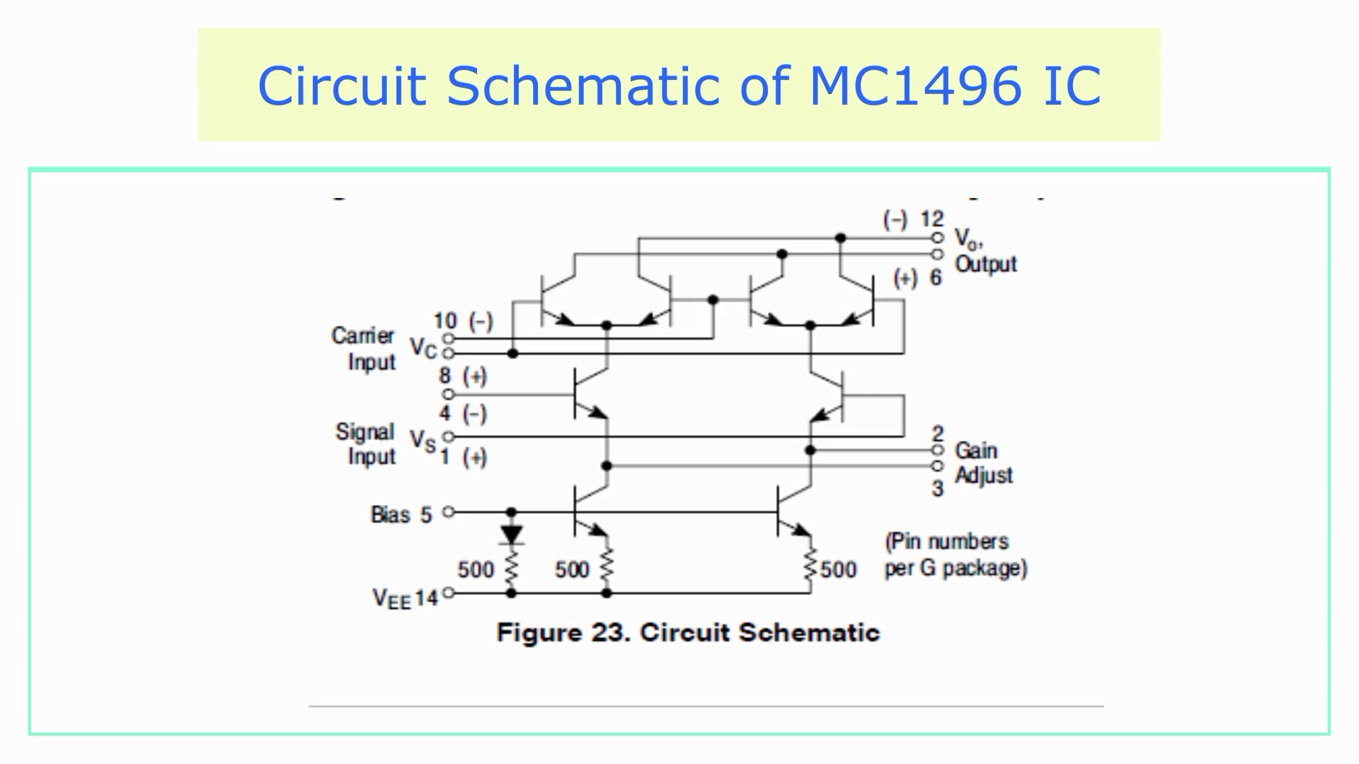
The output spectrum will contain only the sum and difference of the two input frequencies. The lower differential amplifier has the emitters connected to the external IC pins and therefore an external emitter resistance can be used.

MC1496 IC Operational Information
The upper quad differential amplifier may be operated in a linear or a saturated mode, whereas the lower differential amplifier is operated in a linear mode for most applications. The maximum input voltage for linear operation is approximately 25 mV peak with no emitter degeneration and the upper differential amplifier has its emitters internally connected. The lower differential amplifier has the facility for an external emitter resistance and its linear signal handling range may be adjusted by the user. This IC can be operated in a dual power supply as well as a 12V DC supply.

 
The basic application of the MC1496 IC is a balanced modulator with a double sideband suppressed carrier. This IC can also be used as a product detector, doubly balanced mixer, frequency doubler, phase detector and FM detector.

MC1496 IC Used as a Product Detector
The MC1496 IC can be used as an excellent product detector. It has a sensitivity of 3 uV and a dynamic range of 90 dB. The detector is broadband and responds well over the entire high frequency range.
 
 
For operation at lower intermediate frequencies down to 50 kHz, the 0.1uF capacitors on pins 8 and 10 should be increased to 1 uF. The output filter at the 12th pin can be tailored to a specific intermediate frequency or audio amplifier input impedance.

MC1496 IC Circuit Description
The  MC1496 IC product detector circuit is wired onto a PCB. The carrier input of around 300 mV RMS is given to the 10th pin of the IC. The RF signal from the antenna and RF amplifier is given to the 1st pin of the IC. The 14th pin is grounded. The 6th and 12th pins are given +12 volts VCC through a 3K resistor.
 
 
An output audio filter is given at the 12th pin through which the demodulated audio signal can be obtained. The emitter resistance between pins 2 and 3 may be increased or decreased to adjust the circuit gain, sensitivity and dynamic range of the product detector. This circuit may also be used as an AM detector when an AM signal is introduced at the RF input and a carrier signal at the carrier input.

Typical Applications of MC1496 IC are
  1. Carrier suppression.
  2. Amplitude modulation.
  3. Synchronous detection.
  4. FM detection.
  5. Phase detection.
  6. Chopper applications.


Direct Conversion Radio Receiver Using the NE602 IC Double Balanced Mixer Product Detector

NE602/SA602A is a high-performance and low power double-balanced active radio frequency mixer/product detector with an on-chip oscillator, input amplifier and voltage regulator. This mixer/product detector IC contains the Gilbert cell differential amplifier or multiplier, which provides optimal mixer characteristics such as good port-to-port isolation, high gain, higher operating frequency, low noise etc.
 

This mixer provides about 18 dB of gain at 45 MHz. The in-built oscillator operates upto about 200 MHz. The oscillator section can be configured as a variable frequency oscillator, crystal oscillator or as a buffer amplifier for an external local oscillator.
 

The NE602 mixer/product detector IC is superior in terms of gain, intercept performance, low noise and low power characteristics. This IC is available as an 8-pin DIL or SO package.

The Important Features of the NE602 IC are,
  1. Low current consumption of typically 2.4 mA.
  2. Excellent noise figure of less than 5 dB at 45 MHz.
  3. High operating frequency.
  4. Excellent gain, intercept and sensitivity.
  5. Low external parts count, therefore easier to build.

NE602 IC Product Detector Considerations
In this direct conversion receiver, the NE602 IC acts as a product detector. This IC is able to provide high dynamic range, if the input signal levels are not exceeded as specified by the manufacturer. It has the ability to accomodate large signals without degraded intermodulation distortion. A bandpass filter and RF amplifier stage at the input provides enough gain with good signal to noise ratio. The RF input pins and the output pins are biased internally and therefore do not need to bias externally.
 
 
Local oscillator injection level is about 200 mV, which also gives adequate dynamic range and mixer gain. Mixer noise figure comes to around 5 dB at 45 MHz. The output is obtained as an audio signal, which is filtered using a low pass audio filter and amplified by an audio power amplifier.

Circuit Description
The NE602 product detector circuit is wired onto a PCB. An LC tank circuit is attached between the 1st and 2nd pins of the IC. The tank circuit is tuned to the required frequency of operation. The 2nd pin is grounded using a 0.01uF capacitor. The RF input is given through a small value coupling capacitor to the LC tank circuit or through a primary winding on top of the tank circuit.
 
 
The pins 6 and 7 are used for the purpose of an in-built LC oscillator or crystal-controlled oscillator. This in-built oscillator operates upto around 200 MHz. An external local oscillator or VFO signal of about 200mV peak to peak can also be given to the 6th pin of the IC to drive this mixer. The audio output is obtained through the 5th pin through a coupling capacitor. A regulated supply voltage of 6-8 volts is given through the 8th pin of the IC.

Applications of NE602 IC
The NE602 IC is used in applications such as,
  1. Cellular radio mixer/oscillator.
  2. Portable radio systems.
  3. VHF transceivers.
  4. RF data links.
  5. HF/VHF frequency conversion.
  6. Instrumentation frequency conversion.


Monday, October 17, 2022

Direct Conversion Radio Receiver Using the Diode Ring Single Balanced Product Detector

A singly balanced diode ring product detector is a passive radio frequency mixer or product detector that does not need a supply voltage to operate. Here, two diodes are used along with a broadband transformer that utilizes trifilar windings over a ferrite balun core or toroid.
 
 
The diode ring mixers are broadband and operate on a wide range of frequencies. They have relatively lower noise figures as compared to the active mixers. These are also called as balanced mixer/product detectors because it prevents the local oscillator signal from appearing at the RF input or the audio output ports.

Diodes used in the product detector

Toroid cores used in the product detector

The diodes that are commonly used here are the hot-carrier diodes or Schottky diodes, although high-speed silicon switching diodes such as 1N4148 or 1N914 etc. are also used. Detector diodes like the 1N60 were used without much difference in performance. The forward voltage drop across each diode in the ring determines the mixer's drive level required for optimum performance.
 
 
The local oscillator signal must be around 20 dB higher than the RF signal for adequate operation. The characteristics of this product detector like the bandwidth or frequency response depends upon the winding of the transformer, such as the number of turns, distance between the turns, permeability of the core etc.
 

Winding the Broadband Transformer
The broadband transformer utilizes trifilar windings over a ferrite balun core or a toroid core. For high frequency spectrum, ferrite cores of high permeability such as Amidon type FT-37 to FT-43 cores are used.
 
 
A typical transformer consist of 10 turns trifilar windings of #28 or #30 SWG enameled copper wire is wound through a ferrite core or balun core. For VHF or UHF frequencies, cores with still lower permeability such as 125 material or Amidon type FT-61 are used. The local oscillator signal power of about +15 dBm is necessary for optimum performance of this product detector. An RF voltage measured at around 250-300 millivolts is needed to adequately run this mixer/product detector.

Working of the Circuit
The VFO signal is applied at point C, which is the intersection of the two secondary windings of the transformer and the radio frequency choke. A signal at point C drives the two secondary windings of the transformer in opposite directions. As the signal at point C swings to the positive side, the upper diode A conducts, which places a charge at the 0.01uF capacitor. On the negative swing of the signal at point C, the lower diode B conducts, which removes the charge from the capacitor. Therefore, the overall charge becomes zero.
 
 
However, when a carrier signal comes across the transformer from the RF input, one of the diodes conducts earlier or later. It causes an unbalance in the net current flow to the capacitor. This unbalance across the diodes causes a charge to be observed across the capacitor as an audio voltage, which is received at the output.

Circuit Description
This product detector has two input ports and an output port. One of the input ports is for the RF input from the antenna and the other for the local oscillator injection. The detected audio signal is obtained from the output port. The RF signal from the antenna is given at the center tap of the secondary winding of the transformer through a 0.01 uF capacitor. The center tap of the secondary winding is terminated by an RF choke towards the ground. The local oscillator signal is given at the primary winding of the transformer.
 
 
The output of the product detector is obtained from the junction point of the two diodes. A low pass audio filter is given to filter off the RF components from this audio signal. It is then amplified by an audio preamplifier to boost the weak signals before it is further amplified by a power amplifier and fed through the loudspeaker. The hum that is audible at the output can be reduced by attaching a balanced antenna at the input or by connecting about 10 meters of wire, with one end of the wire connected to the circuit ground and the other end spread across the ground.

Disadvantages of the Diode Product Detector
  1. The singly balanced two diode product detectors have an insertion loss of about 5db.
  2. It needs a higher local oscillator drive signal than the active detector, and needs a local oscillator drive of +15dBm.
  3. An audio preamplifier stage is necessary to sufficiently amplify the weak audio signals.


Direct Conversion Radio Receiver Using the CA3028 IC Tuned Single Balanced Product Detector

The CA3028 is a differential amplifier IC that operates at frequencies from DC to 120 MHz, which is used in communication equipment and other industrial applications. CA3028 IC can be used as an active mixer as well as a product detector or demodulator. The mixer and the product detector both have two input ports and an output port. A mixer combines an input signal from the antenna with a locally generated RF oscillator (VFO) signal and creates a frequency shift, shifting the frequency up or down producing an RF or intermediate frequency signal at the output.


A product detector or demodulator on the other hand combines the radio frequency signal input from the antenna or an intermediate frequency signal from the IF stage with a beat frequency oscillator (BFO) to produce a demodulated audio signal at the output. In this DC receiver, the CA3028 IC works as a tuned singly balanced product detector. It is an active device, therefore, it provides a conversion gain.


The CA3028 IC is no longer manufactured, therefore the IC equivalent circuit is used here. The equivalent circuit of the IC is wired onto a PCB to construct the mixer or product detector stage. It is an 8 pin IC and consists of three transistors and three resistors for biasing. Two transistors act as the RF input ports through which RF signals are fed into the mixer and a third transistor acts as the output port where the demodulated audio is obtained.


The Important Features of the CA3028 IC are:
  1. It is controlled for input offset voltage, input offset current and input bias current.
  2. Balanced differential amplifier configuration with controlled constant current source.
  3. Single-ended and dual ended operation.


CA3028 IC Important Features
 
Circuit Description:
The CA3028 IC equivalent circuit with the three transistors is wired onto a PCB. The resonant tank circuit is made using an inductor and a variable capacitor through which it is tuned to the radio frequency that is received. The resonant circuit is attached to the base of one of the input transistors.


The RF input is coupled to the resonant circuit by means of a low value capacitor for eg. 47 pf or below. A local oscillator signal is given to the base of another input transistor. The strength of the local oscillator signal of about 100-300 millivolts is needed to drive this product detector. The detected audio signal is received at the collector of the third transistor. Bypass capacitors are provided to bypass any RF components present at the output stage. The three transistors act as the three ports in this product detector circuit which provide enough isolation between the ports. The detected audio signal is filtered of its RF components using an audio filter and then amplified using a preamplifier stage before it is further amplified by a power amplifier.


In a direct conversion receiver, there is insufficient gain obtained due to the absence of RF or IF stages as in superheterodyne receivers, so most of the gain has to be provided by the audio amplifier. A preamplifier section is usually added to boost the weak audio signals before it is being amplified by the power amplifier. There is a slight hum that is picked up by the detector stage, which is a disadvantage in most DC receivers. This can be reduced by connecting around 10 meters of electrical wire with one end connected to the circuit ground and the entire length of the wire stretched on the ground.

Applications of CA3028 IC
  1. It is used as an oscillator, singly balanced mixer/product detector and limiter in radio receivers.
  2. It is used as RF and IF amplifiers (either in differential or cascode arrangement) in radio and communication receivers.
  3. It is used as DC, audio and sense amplifier.
  4. It is used as a converter in the commercial FM band.


RF Tuner and Amplifier for a Radio Receiver || How to Construct an RF Tuner and Amplifier

An RF tuner and amplifier is a tuning and amplifying section connected to the input of a radio receiver or a communication receiver. The input of this stage is connected to the antenna and the output is connected to an RF mixer.


The addition of this section in a radio receiver is meant to tune and amplify the signals coming from the antenna before it is fed to the RF mixer stage. It helps to improve the gain, sensitivity and selectivity of a receiver.
 

The RF tuner and amplifier has two sections:
1. RF tuner section.
2. RF amplifier section.


RF Tuner:
The RF tuner section consists of a parallel tuned resonant circuit coupled to the antenna and its output is coupled to the RF amplifier stage. The resonant circuit is coupled to the antenna using a small value coupling capacitor. This section helps to tune to a narrow and selected range of frequencies from a wide radio frequency spectrum.
 
 
The higher Q factor of the tuning circuit helps to improve the signal to noise ratio. It helps to select a weak signal of a specific frequency from signals in the adjacent frequencies, thereby helping to avoid overlapping of signals. It prevents noise that is present in the adjacent radio frequency spectrum from entering into the input of a receiver. The quality or Q factor of the input tuned circuit that is tuned to the required frequency in superheterodyne receivers helps to reject the image signals from getting into the mixer stage and causing image interference. The resonant frequency of this parallel tuned circuit is determined by the formula, Fr = 1/2π√LC.
 
RF Amplifier:
This section consists of a common emitter transistor amplifier in a broadband configuration. The output of the RF tuner stage is coupled to the input of the RF amplifier. It amplifies the weak signals from the RF tuner stage and provides an amplified signal at its output. An RF gain control is provided for adjustment of RF gain, that helps to improve the reception of weak signals and it also helps to reduce the gain while receiving strong signals.
 
 
The amplifying device is a small signal low-noise device that has higher operating frequency. A broadband RF amplifier is used here that amplifies a wide range of frequencies covering most of the HF radio spectrum into the VHF range. The input and the output terminals must be sufficiently terminated to allow for maximum transfer of signals. An RF choke is used at the collector of the transistor, through which the output is coupled.

Applications of RF Tuner and Amplifier:

  1. The RF tuner and amplifier is used to selectively amplify weak signals from the antenna in radio and communication receivers.
  2. It is used as an RF preselector at the input of most general coverage radio receivers that helps in the reception of weak signals in the medium frequency (MF), high frequency (HF) and very high frequency (VHF) bands.
  3. It significantly reduces the adjacent signal interference and image reception problems in superheterodyne receivers.
  4. It is used as an input preselector section in radio frequency converters.
  5. It considerably strengthens the signals from the antenna in software defined radios.
  6. It improves sensitivity and selectivity to radio signals in broadcast radio receivers.


Direct Conversion Receiver Using the CA3028 Single Balanced Mixer Product Detector

A direct conversion receiver is a type of radio receiver, which uses an unmodulated carrier frequency of the same frequency as that of the incoming radio frequency signal to mix using a synchronous detection technique and detects the audio or information from the received signal.
 
 
Here the unmodulated carrier frequency is generated by the local oscillator or the VFO. The local oscillator signal mixes with the incoming radio frequency signal and produces a beat note. The circuit is not so complex as compared to the superheterodyne receivers, but it lacks dynamic range. It can demodulate signals in modes such as CW, SSB and digital modes, but cannot detect signals in the AM or FM modes. Direct conversion receiver is also called the homodyne receiver, synchrodyne receiver or zero IF receiver.


Operation of a Direct Conversion Receiver
The signal from the antenna is tuned using a bandpass filter or a tuning circuit, which selectively tunes to the required frequency. A local oscillator signal is generated at the same frequency as that of the incoming radio frequency signal.

 
The incoming signal from the antenna is mixed with the local oscillator signal that is generated by the VFO in an RF mixer. The frequency of the local oscillator signal and the incoming radio frequency signal are the same. These two signals mix with each other in the mixer stage and are converted into a baseband audio signal.
 
 CA3028 IC Internal Configuration
 
 
The RF components are filtered using a low pass audio filter to produce only the audio frequency signal at the output. The modulated RF signal is converted directly to the baseband signal by a single conversion and therefore, it is called the direct conversion, homodyne or zero IF receiver.
 
 
The output audio signal is then amplified using an audio preamplifier and a power amplifier.


Advantages of DC Receivers
  1. A DC receiver does not have the complexity of the superheterodyne receivers such as multiple frequency conversions, multiple IF amplifier stages, image rejection problems etc.
  2. This receiver has high selectivity and therefore, it demodulates the signals quite precisely.
  3. It does not need a separate product detector stage.
 
Disadvantages of DC Receivers
  1. Due to the lack of IF amplifier stages and automatic gain control, the baseband signal strength fluctuates over a wide range. This fluctuation of the baseband signal depends on the strength of the incoming signal.
  2. It demodulates CW, SSB and digital pulsed signals well, but is unable to detect AM or FM signals. It requires phase locking of the local oscillator to the incoming carrier signal, which is more difficult to achieve.
  3. A beat signal is always heard when trying to resolve AM signals in a DC receiver.
  4. There is an audible hum generated in some DC receiver designs.

Applications of DC Receiver
  1. With the development of IC chips incorporated with phase-locked loop circuits, the potential uses extends to demodulation of AM radio signals and other complex modulation techniques.
  2. Direct conversion receivers are used in receiver applications such as software defined radios, cellphones, television, medical imaging, avionics etc.


Saturday, October 15, 2022

Class AB Transistor Audio Power Amplifier || How to Construct a Class AB Audio Power Amplifier

The class AB complementary pair transistor audio amplifier is a configuration that works using the push-pull audio power amplification method. The class AB amplifier is a combination of class A and class B amplifiers. Here, the transistors are biased in such a way that they conduct for more than 180 degrees and less than 360 degrees of the input waveform. It has good distortion-less amplification as well as high DC to AC conversion efficiency.
 
 
The forward voltage drop at the PN junction of 0.7 volts at the transistor base is reduced by biasing the transistors accordingly. Thus the transistors will conduct for more than 50% or 180 degrees of the input cycle. It minimizes the problem of crossover distortion that affects the class B operation. The biasing is done using a voltage divider network or a series connected diode arrangement.

Working of Class AB Audio Power Amplifier
Three transistors are used here to construct this audio power amplifier. Two complementary transistors, one NPN and the other PNP transistors are used as push pull output power amplifiers and another NPN transistor is used as the driver. There are two forward biased diodes in series, which are used to bias the output transistors. A small current constantly flows through the network of resistors and diodes such as R1, D1, D2 and R2 that provides the required voltage for the biasing. When no input voltage is given, the point between the two diodes will remain zero.

As the current flows through the biasing network, there is a forward bias voltage drop of approximately 0.7 volts across the diodes, which is applied to the base-emitter junction of the push pull transistors. The voltage drop across the silicon diodes gives a biasing voltage of 0.7 volts for the NPN transistor and -0.7 volts for the PNP transistor. This constant voltage drop across the two diodes, biases the transistor above the cut-off. There are less biasing voltage changes that can happen due to temperature variation as the electrical characteristics of the diodes are closely matched with that of the base emitter junction of the transistor. This compensates for variations in temperature at the base-emitter junction and thereby helps to prevent crossover distortion. This amplifier provides about 200 mW of power into an 8 ohms load using a 9 volts battery.

Applications of Class AB Audio Amplifier
  1. This amplifier is used for audio amplification in low powered battery operated radio receivers.
  2. It is suitable as an audio amplifier in radio and communication receivers used for portable operation.
  3. The class AB amplifier is preferred in audio amplifiers that have least distortion such as multimedia players, intercoms, TV sound systems, line drivers etc.


Direct Digital Synthesis DDS VFO || Different Parts, Functions and Working

A direct digital synthesis VFO or DDS VFO is a type of variable frequency oscillator, which employs digital frequency synthesizer or clock generator integrated circuits to produce sine waves of a specific frequency. It is run by the Arduino Atmega 328 microcontroller and displays the output through a 16 x 2 LCD display or a Nextion screen. Nowadays, it is widely used in digital communication devices such as radio receivers, transmitters, mobile phones, satellite receivers, set-top box, HDTV, radio control toys and games, WiFi routers, communication gadgets etc. It provides much better frequency stability, improved phase noise and output phase control than the analog VFOs. It also provides a good input interface and a pleasing visual display.


DDS VFO Working with 12 Mhz IF Shift

Parts of a DDS VFO
A DDS VFO consists of two main functional segments, A. The hardware part and B. The software part. The software part gives command to the hardware section to produce sine waves of a specific frequency and perform functions according to the input given. The hardware section works in tandem with the software part to accept the input, generate sine waves and display the readout onto the screen.


A. DDS VFO Hardware:
The hardware part of a DDS VFO consists of various devices and modules that carry out specific functions. Those devices and modules used in the construction of a DDS VFO are as follows:

1. DDS Chip:
The frequency generation of this VFO is done by the direct digital synthesizer chips available as the si5351, si570, AD9850, AD9851 etc. The chip used here is the si5351, an I2C configurable clock generator. It has three different clock outputs, clock 0, clock 1 and clock 2. This chip can generate frequencies from 8 khz to 160 MHz. It needs a supply voltage of 3.3 volts.
 

2. Microcontroller:
Arduino nano: It is a small and complete board based on the ATmega328 single chip microcontroller with a clock speed of 16 MHz. It has an operating voltage of 5 volts. The CPU is composed of the Microchip AVR(8bit). Arduino nano has 30 male input/output headers in a DIP-30 configuration. There are 14 digital I/O pins of which 6 pins provide PWM output and 8 analog input pins. It has 32 KB of flash memory and can be programmed using the Arduino software IDE. The board can be powered using a type-B mini-USB cable or a 9 volt battery. It provides serial data communication, available through the digital pins 0 (RX) and 1 (TX). The onboard LED flashes when the data is being transmitted.


3. Input Devices:
These consist of the rotary encoders, keypads, touchscreens etc. A rotary encoder is an electro-mechanical device, which converts the angular position or motion of a shaft or axle into digital output signals. It uses mechanical, optical or magnetic technology to encode the information. There are two pins on one side, which is used for switching and three pins on the other side, which is for varying the frequency.
 
 
4. Display Screen:
Screens such as the 16 x 2 LCD display or Nextion screen are used for display. The 16 x 2 LCD display has a total of 16 pins. The first pin is connected to the ground, the second pin is given +5 volts, and the third pin is contrast control, through which positive voltage is fed through a 10k preset. Pins 4, 6, 11, 12, 13 and 14 are connected to the Arduino. The 15th pin is given +5 volts and the 16th pin is connected to the ground, these pins are used for LCD backlight.


5. Power Supply:
The voltage for the Arduino nano is 5 volts and it is supplied by the 7805 IC voltage regulator. The direct digital synthesizer chip needs about 3.3 volts to operate, which is obtained from the 17th pin of the Arduino nano board.


B. DDS Software:
The software part of the DDS VFO consists of the Arduino IDE and the DDS VFO software. The latest version of Arduino IDE is installed on the computer. The Arduino Nano is connected to the USB port of the computer. All library files and driver files of the connected hardware are installed. Download a suitable DDS VFO software from the GitHub website. Open Arduino IDE, insert the downloaded DDS VFO program into the IDE. Do the compilation and make sure there are no errors present. Add the required library files if errors are still present on compilation. Edit the lines of code for changing or tweaking up the functions and parameters of the VFO. Upload the program into the Arduino nano. Now the operating frequency and all other parameters become displayed onto the LCD screen.


Working of a DDS VFO
The operation of a DDS VFO is controlled by the Arduino Atmega 328 microcontroller. Various programs and codes for running the VFO are written in the Arduino nano. Necessary commands, reference waveforms and various functions are also stored into the memory. The input devices such as the rotary encoder or keypad are used to feed data such as the VFO frequency, BFO frequency, step size and other functions to the microcontroller.


A crystal oscillator, frequency reference clock is used to create identical waveforms. It operates on fixed crystal frequencies of 25 or 27 MHz. A phase-locked loop section helps to stabilize the output frequency to the generated sine wave. It is multiplied and then divided by a specific number to get the required output frequency. There are three clock outputs available on the DDS chip, one is used for the VFO and another for the BFO.
 
 
The program executes the code and the frequency synthesizer chip generates the waveform according to the input given. The generated frequency waveform is obtained from the clock output. The frequency of operation, BFO frequency, intermediate frequency, step size, memory channels and other functional parameters are displayed onto a 16 x 2 LCD display or a 2.8 inch Nextion screen.

Advantages of the DDS VFO
  1. A DDS VFO has many advantages over the analog VFO. These advantages are,
  2. Frequency stability. It operates by phase-locked loop method and therefore the output has high frequency stability.
  3. Frequency agility. The DDS output frequency is determined by the value stored in the frequency control register, which controls the phase accumulator step size, thereby increasing the frequency agility.
  4. Reduced phase-noise and jitter. The superior phase-noise performance is due to the feed-forward system of the DDS.
Applications of DDS VFO
  1. DDS VFOs are used in modern radio receivers and transmitters.
  2. It is used in household devices and gadgets such as mobile phones, satellite receivers, set-top box, HDTV, radio control toys and games, WiFi routers, communication gadgets etc.
  3. It is used for instrumentation purposes such as signal generators,  oscilloscopes, reflectometers, radars etc.


Variable Frequency Oscillator or VFO and its Functions

A variable-frequency-oscillator is an electronic oscillator whose frequency can be varied or tuned over a range of frequencies and then amplifies the signal that is produced. It is an essential part of a radio receiver or a transmitter. It is a very important component in household equipment such as radio, television, mobile phones, satellite receivers, walkie-talkies, communication devices, radio operated toys etc.

Variable Frequency Oscillator Testing

The VFO produces a waveform in the radio frequency spectrum or even into the audio frequency range depending on the frequency of use. The waveform most commonly used is the sine wave, which is mostly used in communication. There are also other types of waves such as square waves, triangular waves, saw-tooth waves etc.
 
 
The main signal generating stage in a VFO is the oscillator. The variable frequency control and the band selector varies the frequency of oscillator in a VFO. Then there are other stages of the VFO, which buffers, isolates and amplifies the required signal. There are different types of radio frequency oscillators, some of which I have described in my previous videos.


Types of VFO:
There are two main types of VFO that are commonly in use and they are:
1. Analog VFO. The analog VFO uses the LC network to provide feedback in the oscillator. A tuning capacitor or a varactor diode is used to change the frequency of oscillation in an analog VFO.
2. Digital VFO. À digital frequency synthesizer is used to generate the signal in a digital VFO.
The three types of digital VFOs are,
A. Direct digital synthesis (DDS).
B. Direct frequency synthesis (DFS).
C. Phase locked loop (PLL) VFOs.

 
Electrical Characteristics of an LC Oscillator:
The stability of an LC oscillator is of utmost importance in both reception and transmission of radio signals. So, proper design of an LC oscillator helps to provide frequency stability over a wide range of frequencies that it operates. Only an adequate amount of feedback is given that is needed to quickly start the oscillation, provide a pure sine wave pattern and to minimize pulling by external load changes.
 
VFO Circuit Using the Colpitts Oscillator

It is essential to bias the oscillator only to a required power level that is needed to drive the buffer stage, which is about 10 mW of power. Higher oscillator driving power may increase the chances of heat generation and therefore frequency drifting. The selection of components in an oscillator is critical, so those components that have the least temperature change and maintain higher frequency stability are used. BJT transistors with high fT such as 250 MHz must be used and a transconductance of 2000 and higher must be used in an FET. Short leads and mechanical stability are also important parameters in VFO design. Long leads may introduce inductance into the circuit and it also lowers the Q. Mechanical stability helps to hold the VFO components in place and reduce frequency variation. There is also a possibility of oscillator drift that occurs with fluctuation of input voltage. Therefore, a stable power supply is essential for a VFO. VFOs must be sufficiently shielded to prevent external physical factors such as external capacitance, temperature, humidity or external signals to influence its operation. The output of a VFO must be taken out through a shielded wire or a 50 ohm coaxial cable.

Parts of a VFO:
There are four main functional stages in a variable frequency oscillator and they are
1. Oscillator stage: The oscillator is the signal generating stage of the VFO. There are different types of oscillators used in VFO such as the LC oscillators, varactor tuned oscillators, crystal oscillators, phase locked loop oscillators, direct digital synthesis (DDS) oscillators etc. The oscillator stage produces sinusoidal oscillations or sine waves at a specific frequency. The frequency of oscillations are controlled by a variable capacitor, potentiometer or a rotary encoder depending on the type of oscillator.

 
2. Buffer stage. This is a stage that comes between the oscillator stage and the amplifier stage. It acts as a buffer between these two stages, which prevents pulling of the oscillator by subsequent amplifier stages. It also helps in the impedance matching between the input and the output.
 
 
3. Amplifier stage. This is the third stage of the VFO. It selectively amplifies the required signal from the oscillator output. It amplifies the weak signal from the oscillator and feeds it to the next stage. It can also selectively amplify a required harmonic frequency with the use of a tuning network and provides the amplified signal at the output. There may be one or more amplifier stages for amplifying the signal to the optimum level at the output.

 
4. Power supply regulator: The operating voltage for the VFO should be well filtered and regulated. The power supply to the oscillator and the buffer stages are regulated by 6-8 volt zener diodes. The VFO circuit is powered from a well regulated supply using the 7809 IC voltage regulator.


Applications of VFO:
  1. VFOs are extensively used in communication receivers and transmitters.
  2. It is used in household equipment and devices such as broadcast radio receivers, television sets, mobile phones, satellite receivers, walkie-talkies, communication devices, radio operated toys, WiFi routers, connectivity gadgets etc.
  3. It is used for instrumentation purposes such as signal generators,  oscilloscopes, reflectometers, radars etc.